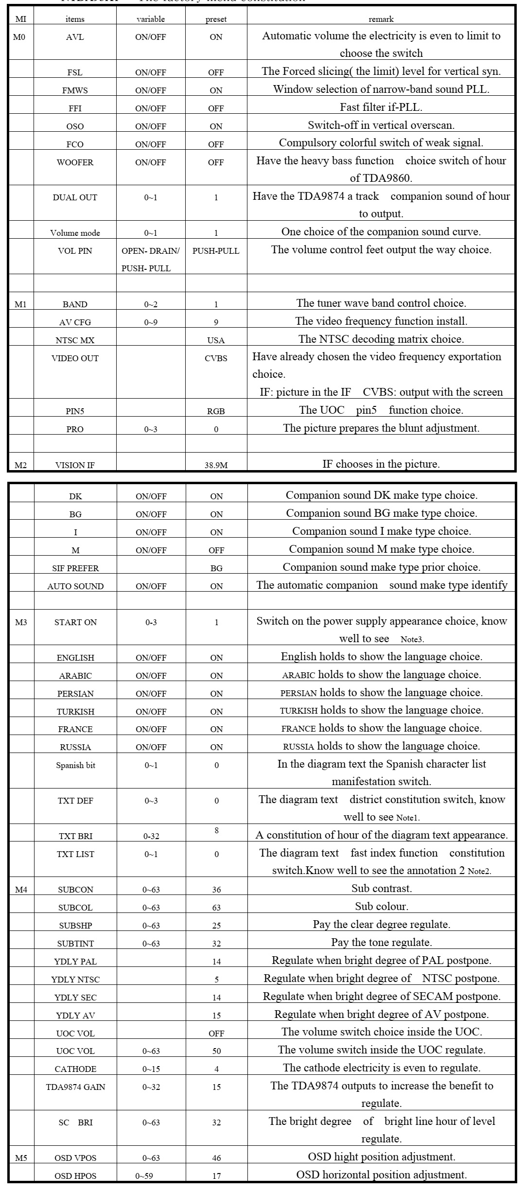
The main chips instruction: TDA93X1
The UOC (“Ultimate One Chip”) TDA93X1 is
adopted in this chassis. This IC is the first available component that contains
the complete control and small signal functionality needed for a TV application
in one device.
The UOC TDA93X1 pins function
description:(total
64 pins)
Pin1: Standby
control,“
1” is on,“ 0” is off.
Pin2: SCL.
Pin3: SDA.
Pin4: Tuning PWM output.
Pin5: Auto AV control SW/NTSC SW,
Pin6: Key board input.
Pin7: Volume
Pin8: Mute control,“ 1” is mute,“ 0” is off.
Pin9: Pin12, Pin18, Pin30, Pin35, Pin41, Pin55: GND.
Pin10: BAND1 control output.
Pin11: BAND2
Pin12: GND
Pin13: SECAM PLL, connected with a
capacitance.

Pin14: +8V power source
supply.
Pin15: Using a capacitor of 220n in series to GND, This pin decouples the
internal digital supply voltage of the video processor and minimizes the
disturbance to the sensitive analogue parts.
Pin16: PHI-2 control loop, this pin requires a capacitor at 2.2nF (C) in series
to GND.
Pin17: PHI-1 control loop, the loop filter connected to pin 17 is suitable for
various signal conditions strong/weak and VCR signal. This is achieved by switching of the loop filter
time constant by changing the PHI-1 output current.
Pin18: GND.
Pin19: Band gap decoupling, the band gap circuit provides a very stable and
temperature independent reference voltage. This reference voltage (4.0 V)
ensures optimal performance of the analogue video processor part of the N301
and is used in almost all functional circuit blocks.
Pin20: East-west pillow signal output.
Pin21: Pin22: Vertical drive output.
Pin23: Pin24: IF input.
Pin25:
Reference current, This pin requires a resistor to ground. The optimal
reference current is 100mA which is determined by this resistor. The 100mA
reference current should not be changed because the geometry processor is
optimised for this current. Furthermore the output current of vertical drive
and EW are proportional to this current.
Pin26: Vertical saw tooth. This pin requires a capacitor to ground of 100Nf
Pin27: AGC output. This
output is used to control (reduce) the tuner gain for strong RF signals.
Pin28: Audio de-emphasis.
Pin29: Sound decoupling. This pin requires a capacitor connected to ground. The
pin acts as a low ass filter needed for the DC feedback loop.
Pin30: GND.
Pin31: Sound loop filter.
Pin32: AVL filter.
Pin33: Horizontal drive signal output needs a resistor in series to +8V.
Pin34: Sandcastle output/fly back input,
Pin35: External audio input, this pin should be grounded in this chassis.
Pin36: EHT tracking/ overvoltage protection. If something is wrong, the anode
high voltage rises, the heater voltage will rise too. When the rising voltage
arrive some limit, the VD461 works, the voltage of pin 36 will exceed 3.9V, the
N301will stop working.
Pin37: PLL loop filter.
Pin38: CVBS output. Monitor or RF videos can be selected.
Pin39: +8V supply source.
Pin40: CVBS input.
Pin42: Y signal input.
Pin43: C signal input.
Pin44: Main audio output
Pin45: RGB signal input blanking.
Pin46, Pin47, Pin48: RGB signal input.
Pin49: ABL. It means been current limiter input. The R464 is the control
resister.
Pin50: Black current input from the CRT board.
Pin51, Pin52, Pin53: RGB drive signal output to the CRT board.
Pin54: +3.3V.
Pin55: GND.
Pin56: +3.3V.
Pin57, Pin58, Pin59: 12MHz crystal.
Pin60:
Reset, NC in this chassis.
Pin61: +3.3V
Pin62: This pin is connected to the HEF4052, Functions expanding.
Pin63: This pin is connected to the HEF4052, Functions expanding.
Pin64: IR signal input.
2 Memory AT24C08 is an E2PROM of 8k, pins describe as follows:
Pin1, Pin2, Pin3,Pin4, Pin7: GND. Pin8: +5V supply.
Pin5: SDA. Pin6: SCL
HEF4052 is described as follows:
total 16 pins

Signal process
The main chip is N301 TDA93X1 AV control switch HEF4052, sound driver is N101 N17821A.
The
TV signal inputs into the tuner (A101) from CABLE or antenna. The pin 10 and
pin 11 of the N301 are combined to select the band. The pin 4 of the N301
outputs the PWM tuning signal. The IF video signal comes from the IF pin of the
tuner. The 38.9MHz IF signal is coupled to the V308 (pre-amplify) and then to
SAWF (Z301). After processed in the SAWF, the 38.9MHz signal gets to the pin 23
and pin 24 of TDA93X1. The IF circuit in TDA93X1 includes such unit as the AGC
amplifying circuit, 38.9MHz oscillator, PLL video demodulator, video amplifier,
IF identify circuit and AFT circuit. The demodulated signal (CVBS) comes from
the pin 38 of TDA93X1, the sound signal comes from the pin 44.The internal CVBS
signal needs norm identification then outputs from the pin 38 of TDA93X1, via
the trap-wave circuit (composed of the V351, Z354, Z352) feeds back to the pin
40 of TDA93X1. The RGB signal comes from the pin51, Pin52, Pin53 of TDA93X1,
and outputs to the CRT board.
The internal sound signal comes from the pin 44 of TDA93X1, via the coupling
capacitor C367 connects to the pin 3 and 5 of TDA9859. The TDA9859 is the audio
effect processor, the AN7522N is the driver. The TDA9859 includes bass, treble,
balance, surround, effect shortcut options.
Through Synchronous separating circuit, the video signal is divided into Horizontal-Synchronizing signal and Vertical-Synchronizing signal. The
horizontal-Sync pulse coming from the pin 33 is transferred to the
horizontal-drive transistor, and will be used to drive the horizontal-transformer.
The horizontal-switch transistor is V451, it and the +B supply drives the flyback transformer to generate the anode high voltage, the focus voltage, the
screen voltage, the CRT board drive voltage 180V, the vertical drive voltage
15V and -15V. The vertical sawtooth wave
is generated on the pin 21 and 22, and then enters the vertical output amplifier
circuit. The vertical output amplifier circuit is realized with the power
amplifier IC –LA78040.
The TDA8177 is a 7 pins vertical deflection circuit (2 Amperes) for DC-coupled
90° or 110° deflection systems with frame frequencies from 50 up to 120 Hz.
Only a single supply voltage for the scan and a second supply for the flyback
are needed.
The vertical drive currents of N301 pins 21 and 22 are connected to input pins
1 and 7 of the TDA8177. The currents are converted into a voltage by resistor
R405. Pin 2 is on a fixed DC level (internal bias voltage, about 2.3V) and on
pin 1 the drive voltage can be measured (typical 1.4 Vpp).
The outputs (pins 4 and 7)
are connected to the series connection of the vertical deflection coil and feedback
resistor R404 and R406. The voltage across R404 and R406. is fed via pin 1 to
obtain a deflection current which is proportional to the drive voltage. The
supply voltage for the TDA8177 is 17V at pin 3. The flyback generator has a
separate supply voltage of V on pin 6. On pin 4 a vertical guard signal is
available. For HF loop stability a damping resistor R407 is connected across
the deflection coil.
Power supply (SMPS)
The IC of KA5Q0765RT is adapted in this chassis; it is the product of
Fairchild. It supplies four DC voltages, one is the +B= 110V, another
is Hcc= 26V, the third is 13V (the sound drive voltage), the fourth is +16V. The +16V can generate the
+8V, +5V and +3.3V by the special generators.
TDA 93X1

AN17821A illustration

TDA8959 illustration

Adjustment method
Main power +B setting
Receive
standard color pattern RF signal, set picture to “ Standard Mode” . Adjust VR501, to get +B
(VD631 -) voltage =110 V
How to enter the factory
mode
With remote controller of factory, continous push [test] key on the remote controller, the TV will hang as fallow:
Normal
> M > BUS OPEN > you can select “M” ( factory mode ) or “normal” mode.
For remote controller of
user
Push [menu] key → display picture manual → push digital key 8500 → display M.
Push
[standby] key, exit factory mode and TV will be standby.
MENU8 Geometrical
adjustment .
Receive standard Crosshatch pattern signal for PAL system .
Horizontal line Shadow
1) Adjust VSLOPE value, to the horizontal line just appear from half bottom shadow.
2) Adjust VSHIFT value, the centre horizontal line correspond to CRT vertical centre.
3) Adjust Vamp value, to get 90% of vertical picture contents would be displayed on CRT.
4) Adjust HSHIFT value, to get the picture horizontal centre correspond to CRT horizontal centre.
5) Receive standard Crosshatch pattern signal for NTSC system, and again
adjust.
MENU7 AGC-TOP adjustment
Receive
60dBu (1mv)VH color bar signal, adjust AGC value(voltage from high to low, to picture
noise reduce gradually to be just disappeared.
MENU9 CRT cut-off and
white balance and sub-brightness adjustment.
Receive
gray and white 2 steps signal.
a) CRT cut off adjustment.
1. push [▲P+][▼P-] key to select “SC”, push [►V+][◄V-] key then automatically
vertical scan will be stopped.
2. adjust SCREEN control on Flyback transformer to get the darkest single
horizontal line (red, green, or blue, sometimes shows
more yellow, more purple or more white).
3. push [V+][V-] key again, vertical scan work repeat.
b) white balance
adjustment.
1. Select RD/BD menu.
2. Adjustment RD/BD to get color temperature as x=281, y=311.
c) Sub-brightness adjustment (use stair case signal)
1. Select SB MENU.
2. Adjust SB to get the darkest step being on or off.
White balance adjustment table